
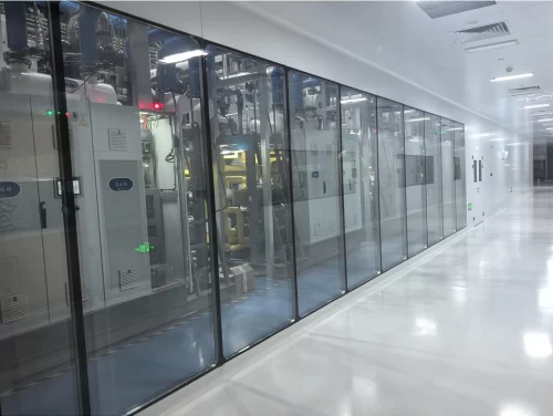
Advanced Microelectronics Enclosures: Eliminating Airborne Micro-Particulates and Structural Vibration
In semiconductor fabrication and photolithography processing, even sub-micron structural vibrations or invisible airborne particulate contamination can result in catastrophic wafer yield losses. Achieving sustained ISO Class 3 to Class 5 (Fed Std 209E Class 10–100) cleanroom environments requires specialized modular enclosures engineered for ultra-low outgassing, strict electrostatic discharge (ESD) dissipation, and vibration-damped structural stability. Partnering with a specialized manufacturer like Farclean allows microelectronics facilities to deploy factory-engineered sandwich panels, anti-static flush doors, and airtight ceiling grids tailored for high-precision chip manufacturing.
Consult Our Semiconductor Cleanroom Engineers Today
Engineering Benchmarks for Class 10–100 Semiconductor Cleanrooms
Advanced semiconductor fabs enforce extreme environmental controls to safeguard nanometer-scale photolithography and wafer alignment processes:
- Structural Vibration Isolation: Enclosure walls and ceiling grids must feature decoupled damping joints to prevent ambient mechanical vibration from compromising sensitive EUV/DUV steppers.
- Comprehensive ESD Control: Wall face sheets and floor coving utilize specialized anti-static powder coatings ($10^6 – 10^9 \ \Omega/sq$) to dissipate static charges instantly and prevent particulate electro-attraction.
- Zero Chemical Outgassing: Non-porous metallic surfaces and specialized silicone-free sealant joinery eliminate volatile organic compounds (VOCs) that fog delicate optics.
Why Leading Fabs Build with Farclean Modular Systems
Farclean eliminates cross-vendor interface risks by manufacturing and delivering integrated modular cleanroom packages built specifically for microelectronics criteria:
1. Precision Modular Panel Damping
Our aluminum honeycomb sandwich panels combine lightweight structural rigidity with inherent acoustic and vibration damping, ensuring stable perimeter enclosures around sensitive fab equipment.
2. Airtight Flush Component Integration
Pre-hung cleanroom doors and flush-mounted double-glazed observation windows eliminate dust-collecting ledges and ensure airtight airlock pressure cascading (15–25 Pa) across process zones.
3. Rapid Deployment with Zero On-Site Contamination
Pre-engineered tongue-and-groove joint systems allow rapid, dust-free assembly on site, shortening facility commissioning schedules by up to 40% compared to traditional construction.
Technical Specifications of Farclean Semiconductor Cleanroom Solutions
The table below summarizes the key technical parameters of Farclean modular enclosure components engineered for high-precision semiconductor environments:
| Modular Module | Farclean Engineering Standard | Performance & Compliance Advantage |
|---|---|---|
| Aluminum Honeycomb Panels | 50mm thick high-density aluminum honeycomb core with ESD powder-coated steel skin | Zero outgassing, Class A fire rating, superior stiffness-to-weight ratio for vibration absorption. |
| Anti-Static Flush Doors | Galvanized steel door leaf with conductively grounded hardware and drop-down bottom seals | Prevents static buildup; maintains strict pressure seals between photolithography and bay zones. |
| Double-Glazed Windows | 5mm+5mm toughened safety glass with anti-static anti-reflective coating and desiccant frame | Flush fit on both sides; condensation-free optical clarity without interrupting laminar airflow patterns. |
| FFU & Ceiling Grid Interface | Integrated T-grid system with liquid gel-seal channel options for ULPA/HEPA filters | Guarantees 99.9995% particulate filtration efficiency at 0.12µm with zero bypass leakage. |
Build Your High-Yield Semiconductor Cleanroom Today
Ensure maximum wafer yield and pass strict ISO 14644-1 Class 3–5 audits with custom modular cleanroom engineering from Farclean. We deliver factory-direct sandwich panels, custom airtight doors, and complete structural designs tailored to your microelectronics layout.
Ready to elevate your semiconductor cleanroom performance? Contact our technical team today to submit your facility specifications and receive a customized 2D/3D design layout and factory-direct proposal within 24 hours.