
Semiconductor Cleanroom Systems: Dust-Free & Anti-Static Panels
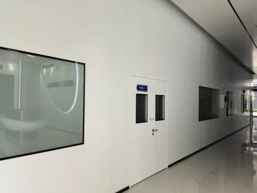
Semiconductor Cleanroom Systems: Dust-Free & Anti-Static Wall Panels and High-Efficiency Partition Systems
For semiconductor manufacturing facilities requiring ultra-clean process environments, the question of cleanroom construction specifications and cost-effectiveness is paramount. Advanced IC fabrication and wafer processing facilities demand specialized cleanroom systems designed to minimize contamination—affecting yield, reliability, and product quality.
While semiconductor-grade cleanrooms range from $1,000 to $10,000+/sqm depending on classification level, our tailored solutions combine cost effectiveness with the highest purity standards. Focusing particularly on Dust-Free and Anti-Static Modular Wall Panels compliant with ISO 14644, ESD protection, and stringent airflow management protocols, our systems meet ISO 14644-1 Class 3-8, ISO 14644-4, and 21 CFR Part 211 requirements.
In this guide, we’ll break down the key specifications, materials, and cost considerations for semiconductor cleanroom construction while highlighting our specialized product offerings for microelectronics manufacturing environments.
1. ISO 14644 Compliant Cleanroom Specifications
ISO 14644-1 and ISO 14644-4 set the global standard for cleanroom classification in semiconductor fabrication. Unlike pharmaceutical GMP facilities, chip manufacturing requires exponentially more stringency due to the nanoscale dimensions of devices. Here’s the classification breakdown:
| ISO Cleanroom Classification | Equivalent Standard | Max Particulate Count (per m³) | Standard Purge Airflow Rate |
|---|---|---|---|
| ISO Class 1 | Class 1 (ISO 14644) | ≤ 10 particles ≥ 0.1μm | ≥ 60 m³/s purge |
| ISO Class 2 | Class 10 (ISO 14644) | ≤ 100 particles ≥ 0.1μm | ≥ 50 m³/s purge |
| ISO Class 3 | Class 100 (ISO 14644) | ≤ 1,000 particles ≥ 0.1μm | ≥ 30 m³/s purge |
| ISO Class 4 | Class 1,000 (ISO 14644) | ≤ 10,000 particles ≥ 0.1μm | ≥ 25 m³/s purge |
These classifications directly correlate with different stages of semiconductor manufacturing—from pre-cleaning and chemical deposition to photolithography and final wafer inspection.
2. Floor-to-Ceiling Cleanroom System Components
To maintain the required purity levels for semiconductor processing, a complete “system” approach is essential:
A. Dust-Free & Anti-Static Wall Panel Systems
Our specially-engineered panels employ advanced filtration technologies to prevent the release of particles—critical for semiconductor processing where even one particle can cause wafer defects or bridge connections:
- FFU-Integrated Panels: Our panels feature removable high-efficiency filter elements (EUROVENT ISO or ULPA grade) that meet ISO 14644-4 requirements, with minimal particle shedding (<1 particle/cm²/week)
- Anti-Static Integration: All conductor-grade materials are properly grounded with controlled surface resistivity (<10^6 ohms/sq.ft.) to prevent electrostatic discharge (ESD) damage to sensitive semiconductor components
B. Cleanroom HVAC & Air Filtration Systems
Advanced semiconductor facilities require specialized air conditioning systems with:
- HEPA/HVIA filters certified for ISO class 1-4 environments
- Proportional damper controls with cascade pressure management
- Temperature stability ±0.5°C & RH stability ±5%
C. Advanced Portal & Airlock Systems
To prevent cross-contamination between process areas:
- High-Efficiency Airlocks: Self-cleaning double-leaf interlocking doors with HEPA-filtered pressure cascade systems
- Portal Decontamination Stations: Optional UV/Ozone sterilization stations integrated with air showers
D. Environmental Monitoring Solutions
Comprehensive monitoring systems include:
- Laser particle counting systems (0.1-10μm range)
- Multi-zone differential pressure sensors
- Surface particle monitoring with Class 100 equivalent pickup kits
3. Cost Considerations for Semiconductor Cleanroom Construction
Construction costs for semiconductor cleanrooms depend primarily on:
A. ISO Classification & Containment Level
Though generally more economical than pharmaceutical cGMP facilities, semiconductor cleanrooms still exhibit significant price variation based on classification:
- Class 1/2: $1,500-$4,000+/sqft
- Class 3-4: $1,000-$2,500/sqft
- Class 5-8: $700-$1,500/sqft
B. Wall Panel Materials Specifications
Materials must balance strength, insulance, and particle containment, with characteristics important for microelectronics:
- Permeability resistance (<5% surface particle pickup rate)
- Chemical resistance to photomasks, acids, and plating solutions
- Dimensional stability under temperature fluctuations
4. FARCLEAN Specialized Solutions
Our proprietary systems are designed with semiconductor manufacturing requirements as the primary consideration:
- Dust-Free Wall Panels: Patented low-shed core technology for laser-cleanroom installations at wafer fabs, ensuring Class 100 equivalent surface particle counts
- Anti-Static System Integration: Comprehensive grounding paths throughout wall panels, doorframes, and ceiling systems to prevent tribocharging in environments processing dynamic semiconductor devices
- Microwave-Cured Silicone Sealants: Specialized edge-seal formulations that resist bond-line delamination in processes using plasma etching gases, ensuring hermetic cleanroom containment
FARCLEAN integrates engineering and manufacturing capabilities to deliver turnkey cleaning infrastructure, including custom-engineered Air Locks, pair-controlled Gateways, and Environmental Control Units optimized for semiconductor manufacturing protocols.
5. Contact FARCLEAN for Semiconductor-Specific Cleanroom Solutions
Our engineering team specializes in creating semiconductor-grade environments for chip manufacturing—from research labs and prototyping facilities to full-scale fab cleanrooms. With comprehensive expertise in ISO 14644 standards and semiconductor ESD protection requirements, we facilitate cleanroom installation in key industry centers including Shanghai Pudong, Suzhou Industrial Park, and Singapore’s East Coast Park Technology Parks.
FARCLEAN (Farce Cleaner) delivers integrated, factory-direct cleanroom solutions for high-purity processing worldwide, with technical support and installation expertise certified by ISO 14644 testing organizations.