
Turnkey Cleanroom Solutions for Semiconductor Manufacturing
The semiconductor industry demands the highest levels of cleanliness, precision, and environmental control. Even microscopic particles can lead to defects in wafers or integrated circuits. To meet these stringent requirements, turnkey cleanroom solutions provide a seamless way to plan, build, and operate contamination-controlled facilities that comply with ISO 14644 standards.
What Is a Turnkey Cleanroom Solution?
A turnkey cleanroom solution means that a single provider handles every stage of the project — from initial design and engineering to installation, validation, and handover. This ensures consistency, faster project delivery, and lower total costs.
- Design & Consultation: Layout planning, airflow simulation, ISO classification selection
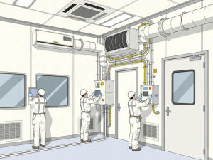
- Engineering & Construction: Modular panels, HVAC systems, filtration, lighting, flooring
- Validation & Commissioning: ISO 14644 testing, documentation, and certification
- Maintenance & Support: Routine checks and performance optimization
Why Semiconductor Manufacturing Requires Cleanrooms
Semiconductor fabrication (wafer processing, lithography, and packaging) involves ultra-fine geometries measured in nanometers. Contaminants like dust, static electricity, or moisture can cause defects or yield loss.
Cleanrooms in semiconductor facilities maintain strict control over particle levels, temperature, and humidity to ensure precision and reliability during every production stage.
Typical Cleanroom Standards for Semiconductor Production:
| Process | Recommended ISO Class |
|---|---|
| Photolithography | ISO Class 4–5 |
| Wafer Cleaning & Etching | ISO Class 5–6 |
| Packaging & Assembly | ISO Class 6–7 |
| Inspection & Testing | ISO Class 7–8 |
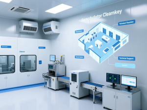
Key Components of a Turnkey Cleanroom Project
- Modular Cleanroom Panels: Easy to install and customize, offering flexibility for future upgrades.
- Air Handling Units (AHU) and HEPA/ULPA Filters: Maintain particle-free environments.
- HVAC Systems: Regulate temperature, humidity, and pressure differentials.
- Lighting & Electrical Systems: Energy-efficient, glare-free illumination for precision tasks.
- Monitoring Systems: Real-time control of environmental parameters.
Advantages of Choosing a Turnkey Cleanroom Provider
- ✅ One-stop solution from design to delivery
- ✅ Reduced project risk and faster completion time
- ✅ Guaranteed ISO compliance and performance validation
- ✅ Simplified communication and project management
- ✅ Lower lifecycle cost through integrated systems
Partner with a Professional Cleanroom Manufacturer
Our engineering team specializes in turnkey cleanroom design and construction for semiconductor and electronics industries. With over 10 years of experience, we deliver solutions that meet international standards while optimizing cost and performance.
Whether you need an ISO Class 5 wafer fab cleanroom or a Class 7 packaging area, we provide complete support — from design to after-sales service.