Semiconductor Cleanroom Project | Turnkey Engineering & Design Solutions
Semiconductor Cleanroom Project — Typical Engineering Solution
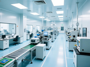
The following is a typical engineering solution for a semiconductor cleanroom project, designed to showcase Farclean’s design capabilities and engineering expertise. All project parameters are illustrative and can be customized according to client requirements.
Project Overview
- Industry Focus: Semiconductor / IC Manufacturing
- Typical Cleanliness Level: ISO 14644 Class 100–1000
- Illustrative Area: 2,000㎡ (scalable according to client needs)
- Core Systems: HVAC, FFU, HEPA/ULPA filters, air shower, pass box, cleanroom panels, monitoring system
- Scope: Design → Materials Selection → Layout Planning → Engineering Simulation → Commissioning Guidance
Design Highlights of This Typical Semiconductor Cleanroom
1. ISO 14644 Airflow & Contamination Control
The design demonstrates a stable laminar airflow distribution to minimize turbulence and maintain low particle levels in critical areas. Key features include:
- ULPA / H14 HEPA filtration
- Intelligent pressure differential control
- Optimized return-air channels for rapid particle removal
2. Temperature & Humidity Stability
To meet lithography and deposition process requirements, the typical solution can achieve:
- Temperature control ±0.2°C
- Humidity control 40%–50% RH
- Localized micro-environment control for critical coating zones
3. Electrostatic & Molecular Contamination Control
- ESD flooring and anti-static construction materials
- Active molecular contamination (AMC) filtration
- Control of organic vapors for stable chip manufacturing processes
4. Modular Hardwall & Softwall Combination
The hybrid structure balances high cleanliness with flexible equipment layout. Modular panels and reinforced aluminum profiles ensure long-term durability.
Installed Systems & Equipment (Illustrative)
- Multi-zone FFU layout for wafer, coating, exposure, and etching zones
- HEPA / ULPA high-efficiency filtration system
- Air showers & pass boxes for safe personnel/material transfer
- Environmental monitoring system for particles, pressure, temperature, and humidity
- High-static pressure HVAC system supporting 24/7 operation
Why Choose Farclean for Semiconductor Cleanroom Projects
- Over 15 years of cleanroom engineering experience in semiconductor industry
- Full turnkey services: design → modular construction → system integration → commissioning guidance
- Customizable solutions to match process, cleanliness, and space requirements
- Documentation and compliance support for global clients
Planning a semiconductor cleanroom? Explore our turnkey solutions and engineering support.

